The following was issued as a joint announcement from MIT.nano and the MIT Research Laboratory for Electronics; CubicPV; Verde Technologies; Princeton University; and the University of California at San Diego.
Tandem solar cells are made of stacked materials — such as silicon paired with perovskites — that together absorb more of the solar spectrum than single materials, resulting in a dramatic increase in efficiency. Their potential to generate significantly more power than conventional cells could make a meaningful difference in the race to combat climate change and the transition to a clean-energy future.
However, current methods to create stable and efficient perovskite layers require time-consuming, painstaking rounds of design iteration and testing, inhibiting their development for commercial use. Today, the U.S. Department of Energy Solar Energy Technologies Office (SETO) announced that MIT has been selected to receive an $11.25 million cost-shared award to establish a new research center to address this challenge by using a co-optimization framework guided by machine learning and automation.
A collaborative effort with lead industry participant CubicPV, solar startup Verde Technologies, and academic partners Princeton University and the University of California San Diego (UC San Diego), the center will bring together teams of researchers to support the creation of perovskite-silicon tandem solar modules that are co-designed for both stability and performance, with goals to significantly accelerate R&D and the transfer of these achievements into commercial environments.
“Urgent challenges demand rapid action. This center will accelerate the development of tandem solar modules by bringing academia and industry into closer partnership,” says MIT professor of mechanical engineering Tonio Buonassisi, who will direct the center. “We’re grateful to the Department of Energy for supporting this powerful new model and excited to get to work.”
Adam Lorenz, CTO of solar energy technology company CubicPV, stresses the importance of thinking about scale, alongside quality and efficiency, to accelerate the perovskite effort into the commercial environment. “Instead of chasing record efficiencies with tiny pixel-sized devices and later attempting to stabilize them, we will simultaneously target stability, reproducibility, and efficiency,” he says. “It’s a module-centric approach that creates a direct channel for R&D advancements into industry.”
The center will be named Accelerated Co-Design of Durable, Reproducible, and Efficient Perovskite Tandems, or ADDEPT. The grant will be administered through the MIT Research Laboratory for Electronics (RLE).
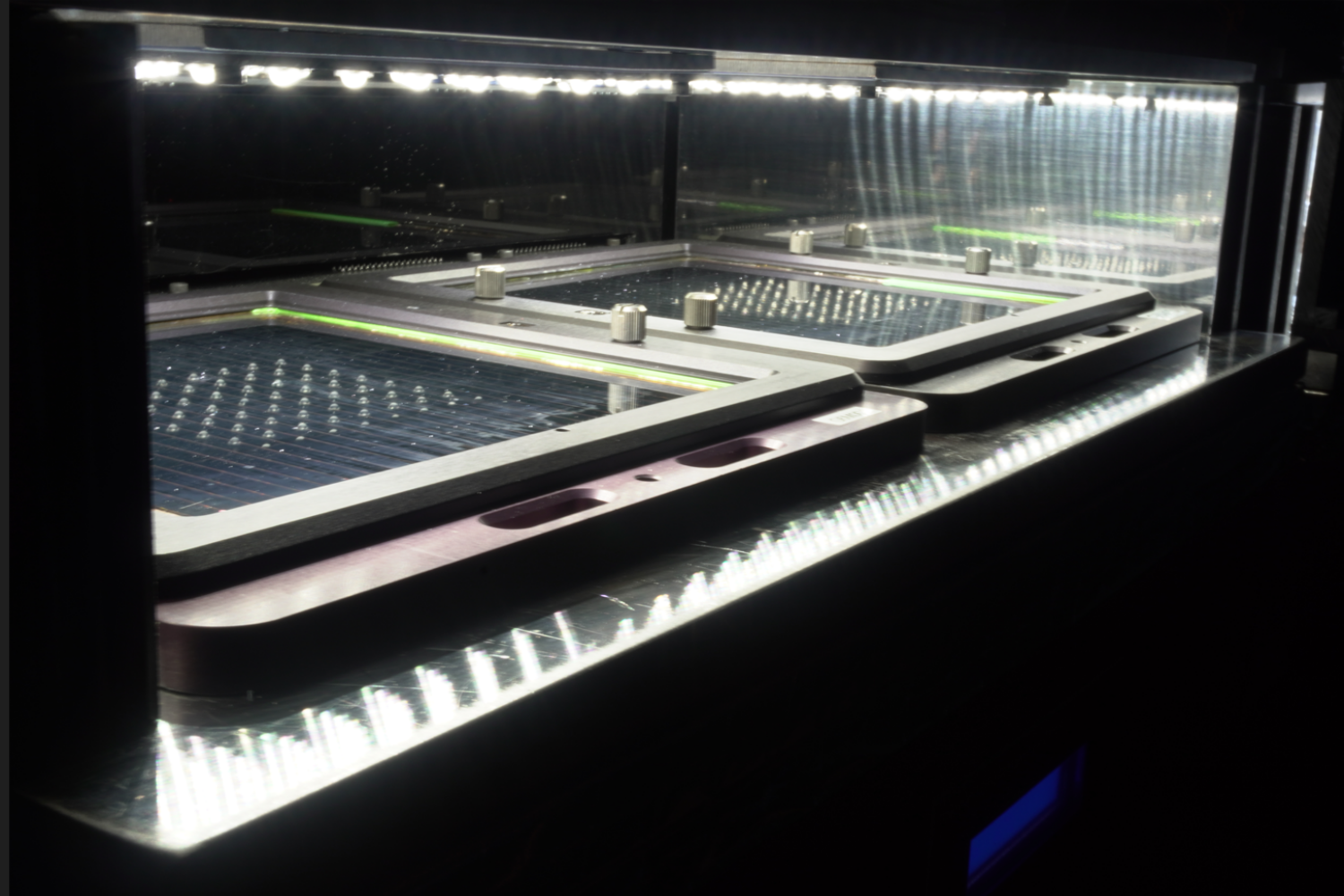
David Fenning, associate professor of nanoengineering at UC San Diego, has worked with Buonassisi on the idea of merging materials, automation, and computation, specifically in this field of artificial intelligence and solar, since 2014. Now, a central thrust of the ADDEPT project will be to deploy machine learning and robotic screening to optimize processing of perovskite-based solar materials for efficiency and durability.
“We have already seen early indications of successful technology transfer between our UC San Diego robot PASCAL and industry,” says Fenning. “With this new center, we will bring research labs and the emerging perovskite industry together to improve reproducibility and reduce time to market.”
“Our generation has an obligation to work collaboratively in the fight against climate change,” says Skylar Bagdon, CEO of Verde Technologies, which received the American-Made Perovskite Startup Prize. “Throughout the course of this center, Verde will do everything in our power to help this brilliant team transition lab-scale breakthroughs into the world where they can have an impact.”
Several of the academic partners echoed the importance of the joint effort between academia and industry. Barry Rand, professor of electrical and computer engineering at the Andlinger Center for Energy and the Environment at Princeton University, pointed to the intersection of scientific knowledge and market awareness. “Understanding how chemistry affects films and interfaces will empower us to co-design for stability and performance,” he says. “The center will accelerate this use-inspired science, with close guidance from our end customers, the industry partners.”
A critical resource for the center will be MIT.nano, a 200,000-square-foot research facility set in the heart of the campus. MIT.nano Director Vladimir Bulović, the Fariborz Maseeh (1990) Professor of Emerging Technology, says he envisions MIT.nano as a hub for industry and academic partners, facilitating technology development and transfer through shared lab space, open-access equipment, and streamlined intellectual property frameworks.
“MIT has a history of groundbreaking innovation using perovskite materials for solar applications,” says Bulović. “We’re thrilled to help build on that history by anchoring ADDEPT at MIT.nano and working to help the nation advance the future of these promising materials.”
MIT was selected as a part of the SETO Fiscal Year 2022 Photovoltaics (PV) funding program, an effort to reduce costs and supply chain vulnerabilities, further develop durable and recyclable solar technologies, and advance perovskite PV technologies toward commercialization. ADDEPT is one project that will tackle perovskite durability, which will extend module life. The overarching goal of these projects is to lower the levelized cost of electricity generated by PV.
Research groups involved with the ADDEPT project at MIT include Buonassisi’s Accelerated Materials Laboratory for Sustainability (AMLS), Bulović’s Organic and Nanostructured Electronics (ONE) Lab, and the Bawendi Group led by Lester Wolfe Professor in Chemistry Moungi Bawendi. Also working on the project is Jeremiah Mwaura, research scientist in the ONE Lab.
#Machinelearning
According to Hacker.top Team researched from news.mit.edu
